PCB Design Course in Pune: Fees, Syllabus & Jobs 2026
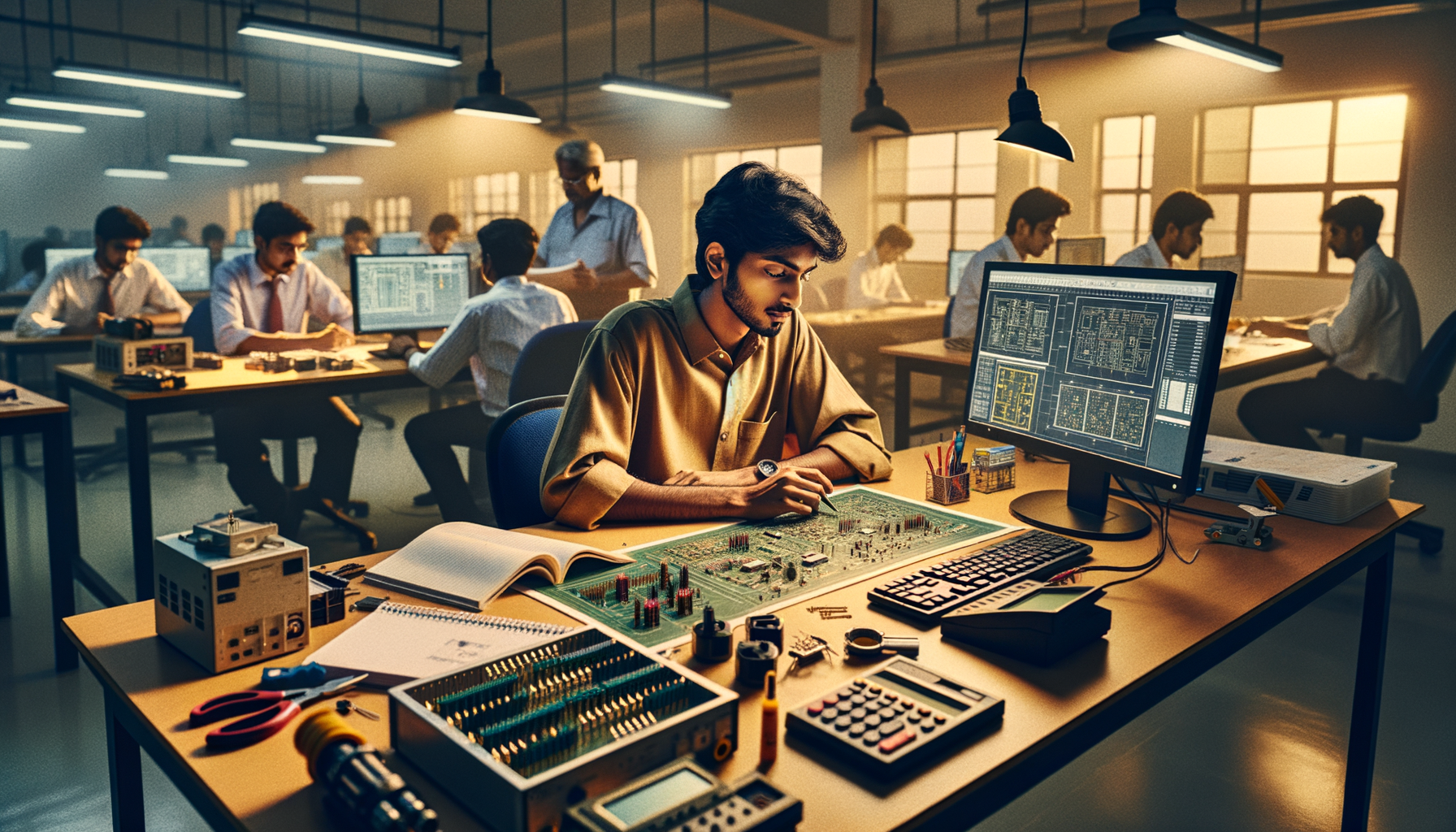
If you're searching for a PCB design course in Pune, you're probably asking the right questions already: how much are the fees, how long does the course take, what software should you learn, and will it actually help you get a job? Here's the thing — PCB design is one of those skills that looks niche from the outside, but inside the electronics industry, it's a serious career path. Companies building automotive electronics, industrial controllers, EV systems, IoT devices, and consumer products all need PCB designers who can work with real tools and real constraints.
I've trained students and working engineers for years, and trust me, the biggest mistake people make is choosing a course based only on fees. What most people don't realize is that software exposure, layout practice, manufacturing file generation, and interview preparation matter just as much as the certificate.
What is covered in a PCB design course in Pune?
A good PCB design course should start from electronics design basics and move into actual board development workflow. For freshers, the syllabus usually begins with electronic components, package types, schematic creation, PCB footprint basics, and design rules. Then it moves into routing, layer stack-up, copper pours, Gerber generation, BOM preparation, and manufacturing checks.
For diploma, BE, BTech, and working professionals, the course should also include signal integrity basics, EMI/EMC awareness, high-speed routing concepts, differential pair basics, grounding strategy, and design for manufacturability. If the training center skips these topics completely, it's too basic for current industry needs.
A practical syllabus in Pune usually includes:
- Electronic components and symbols
- Schematic capture workflow
- PCB footprint creation
- 2-layer and 4-layer PCB layout
- Design Rule Check and Electrical Rule Check
- Manual routing and auto-routing use cases
- Gerber, drill, pick-and-place, and fabrication outputs
- BOM and documentation
- Mini project and industry drawing standards
PCB design course fees in Pune: how much does it cost?
Course fees in Pune depend on software, depth, and whether the training is beginner-level or industry-focused. For a general PCB design course using mixed tools or entry-level software, fees usually fall between ₹18,000 and ₹35,000. If the course includes advanced tools like Altium Designer or Cadence Allegro, project work, and placement support, fees can go from ₹35,000 to ₹65,000.
Short-term crash courses may look cheaper at ₹12,000 to ₹18,000, but many of them cover only schematic and basic routing. The good news is that if you're serious about getting hired, a slightly higher fee for proper lab practice and job-oriented assignments is usually worth it.
In Pune, I've seen students from areas like Kothrud, Hadapsar, Pimpri-Chinchwad, Nigdi, and Wagholi compare only the price. Don't do that. Compare software access, trainer quality, project depth, and whether you'll build boards that can be shown in interviews.
How long is a PCB design course in Pune?
Most PCB design courses run for 6 to 12 weeks if you're attending regular weekday or weekend batches. Fast-track programs may finish in 4 to 6 weeks, while advanced job-oriented modules can continue for 3 to 4 months with project work.
Freshers usually do better in an 8 to 10 week format because they need time to understand schematic thinking, component placement logic, and routing discipline. Working engineers often prefer weekend batches over 2 to 3 months. That's a better pace if you're already in production, testing, embedded, or maintenance roles and want to shift into hardware design.
Which PCB design software should you learn in 2026?
This is where the real comparison starts. Different companies use different PCB tools, and your choice should depend on your career target.
KiCad
KiCad is free, popular, and excellent for learning fundamentals. It's a strong starting point for freshers, hobbyists, startup teams, and students building academic or IoT projects. The learning curve is moderate, and since there's no license cost, it's perfect if you want to practice from home.
Best for: freshers, students, self-practice
Cost: Free
Learning curve: Easy to moderate
Job demand: Moderate, better in startups and small design teams
Altium Designer 24
Altium is one of the most practical tools for professional PCB design teams. It offers strong schematic capture, layout, libraries, 3D visualization, and documentation in one environment. Many hardware product companies prefer it because it's efficient for medium to advanced board design.
Best for: serious job seekers, design engineers, experienced professionals
Cost: High commercial license
Learning curve: Moderate
Job demand: High in product design and embedded electronics companies
Cadence OrCAD and Allegro X
Cadence tools are common in larger organizations and advanced PCB environments, especially where complexity is higher. OrCAD is often used for schematic and PCB flow, while Allegro is preferred for complex boards, constraint-driven design, and enterprise-level design environments.
Best for: experienced learners, engineers targeting larger companies
Cost: High commercial license
Learning curve: Moderate to steep
Job demand: Very high in automotive, industrial, and high-reliability electronics
Autodesk Eagle
Eagle still appears in some academic and startup setups, though it's not the first choice for every company now. It's easier to start with than heavy enterprise tools, but long-term job demand is lower compared to Altium and Cadence.
Best for: beginners, makers, simple board projects
Cost: Subscription-based
Learning curve: Easy
Job demand: Limited compared to Altium and Cadence
Which software is best for freshers vs experienced engineers?
For freshers, I'd say start with KiCad or Altium basics. Why? Because you need to understand placement, routing, footprints, net classes, and output files without getting overwhelmed. KiCad helps you build confidence. Altium gives you better industry alignment if your institute provides proper lab access.
For experienced engineers moving from testing, embedded C, production, or service roles, Altium Designer or Cadence OrCAD/Allegro makes more sense. These tools are closer to what recruiters ask for in Pune, Bengaluru, Chennai, and Hyderabad.
Trust me, software alone won't get you hired. Your board design logic, documentation quality, and interview explanation matter more than just saying, “I know Altium.”
Which companies use PCB design software in India?
In and around Maharashtra, electronics and engineering employers may use different tools based on their product type. Companies such as Bosch, Siemens, Tata Technologies, KPIT Technologies, Mahindra Engineering, Bajaj Auto, Thermax, Kirloskar, and L&T work on automotive, industrial, controls, embedded, and product engineering domains where PCB design exposure is valuable. IT service companies like Infosys and TCS may also have engineering services divisions supporting electronics design, validation, and documentation projects.
What most people don't realize is that recruiters don't always mention every tool in the job title. A posting may say hardware design engineer, PCB layout engineer, embedded hardware engineer, or electronics design engineer. But inside the role, they expect understanding of schematic tools, PCB layout flow, and manufacturing outputs.
What job opportunities are available after a PCB design course?
After completing a PCB design course in Pune, common entry-level roles include:
- PCB Layout Engineer
- Hardware Design Engineer
- Electronics Design Engineer
- Embedded Hardware Support Engineer
- CAD Engineer - PCB
- Component Library Engineer
Freshers in Pune typically start around ₹2.4 lakh to ₹4.2 lakh per year depending on software skills, project quality, and interview performance. With 2 to 4 years of solid experience, salaries often move to ₹4.5 lakh to ₹8 lakh per year. Engineers with stronger Cadence or advanced Altium exposure in automotive or industrial electronics can go beyond that.
If you're open to moving beyond Pune into Chakan, Hinjawadi, Talegaon, Mumbai, Nashik, Aurangabad, Bengaluru, or Chennai, opportunities improve even more.
How do you choose the right PCB design institute in Pune?
Look at five things: software access, trainer experience, project practice, placement guidance, and whether the syllabus includes manufacturing outputs. A proper institute should let you work on mini projects, create libraries, route complete boards, and explain design decisions clearly.
ABC Trainings is one of the institutes students consider when they want practical CAD and electronics-oriented learning with job focus in Maharashtra. If you want details about PCB design training, batch timing, or fees, you can call 8698270088 or WhatsApp 7774002496.
Here's the thing — the best course is not the cheapest one. It's the one that helps you sit in an interview and confidently explain why you placed a connector a certain way, why you used a ground plane, and how you generated Gerber files correctly.
Is PCB design a good career in Pune in 2026?
Yes, especially if you combine PCB design with embedded systems, electronics testing, or product development understanding. Pune has a strong ecosystem in automotive, manufacturing, industrial automation, and engineering services. That creates demand for engineers who can support hardware development and documentation.
The good news is that PCB design is still a skill-based field. If you build genuine hands-on ability, your portfolio can speak louder than marks. That's why students from Pune, Chhatrapati Sambhajinagar, and Sangli often choose project-based training over theory-heavy classroom learning.
What is the fee for a PCB design course in Pune?
In Pune, PCB design course fees usually range from ₹18,000 to ₹35,000 for basic to intermediate training. Advanced programs with Altium or Cadence exposure, projects, and placement support can go up to ₹65,000. Always check what software, lab hours, and project work are included before comparing fees.
Which PCB design software is best for freshers in India?
For freshers, KiCad is a very good starting point because it's free and easy to practice at home. If your institute provides licensed lab access, Altium Designer is even better for job alignment. Start with fundamentals first, then move to industry-level tools once your basics are clear.
Can I get a job in Pune after a PCB design course?
Yes, you can apply for roles like PCB Layout Engineer, Hardware Design Engineer, and Electronics Design Engineer after completing a practical course. Your chances improve if you have mini projects, design files, Gerber outputs, and clear interview explanations. Pune has opportunities in automotive, embedded, industrial, and engineering services companies.
How much salary does a PCB design fresher get in Maharashtra?
A PCB design fresher in Maharashtra usually starts between ₹2.4 lakh and ₹4.2 lakh per year, depending on software knowledge and project quality. Candidates with Altium or Cadence exposure and strong electronics basics may get better offers. Salaries are generally stronger in Pune, Mumbai, and major electronics hiring clusters.
Visit Our Centers
Pune
Wagholi Branch
1st Floor, ABC Trainings, Laxmi Datta Arcade, Pune - Ahilyanagar Hwy, Wagholi, Pune, Maharashtra 412207
Hadapsar Branch
Bloom Hotel, ABC Trainings 1st Floor, S.no 156/3 Shree Tower Pune - Solapur Rd, Hadapsar, Pune, Maharashtra 411028
Start Your Career Journey Today
Join 10,000+ students who transformed their careers with ABC Trainings.
💬 WhatsApp: 7774002496📞 Call: 8698270088